SFP Media Buddy and why SERDES is painful Post
Starting with a UART converter for SFP modules
The initial request
This story, as most of my stories, starts with a reasonable request from a reasonable person.
.
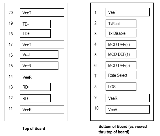
For reference the SFP-UART is a non-standard pinout for SFP and SFP+ modules to allow interacting with what is often a linux kernel on the stick. This does not apply to all SFP modules and mostly just modules intended to work as Passive Optical Network or PON sticks. Much more information on this and the wide range of sticks can be seen at gpon-hack wiki. So first I had to understand what was required for this circuit board. To start off, I had to understand what was required for this circuit board. If we look at the standard SFP socket we get the following pinout:

Pins 11-20 are dealing with SERDES, which is the high speed communication protocol the SFP modules use to talk to the computer. You have VeeT/R which is ground and VccT/R which is 3.3v in this case. The other pins are differential lines for communication.
Pins 1-10 are the interesting ones for SFP-UART. You once again have Vee, which is ground, at 1 and 10. 9 is ground here, but could also be a rate select.
LOS or RxLos is loss of signal Rx at pin 8 and is used by some host to stop all communication with the module
Pin 7 is Rate Select but often unused
Pins 4-6 are "MOD-DEF" or pins defined by the module. Standard however require pins 4 and 5 are SDA and SCL respectively. These are used by the computer or networking gear to identify the module and get status updates such as link status, temperature, and other important information.
Pin 2 is Tx_Fault, along with pins 4 and 5, allows the host to see if there is an issue.
Pin 3 allows the host to disable transmit of the module, but it can also be used by the module to signal its not currently transmitting.
So, how can you get UART out of any of these? The answer is simple
ignore the standard that I eluded to earlier. It turns out the majority of these PON SFP modules repurposed the Tx_Fault pin and Rate Select pin as TX and RX respectively, better known as the Huawei pinout. Another example is pins 3 and 6 , add commaknown as the Nokia pinout.
The Design Phase
With that background information in place, it was time to start designing the actual circuit board.Initially I took pins from pins 1-10 and broke them out with to two analog muxes going into a cp2102 for UART to USB, allowing any pin to be TX and any pin to be RX. I also added were leds to show which pins were selected and if it was active or not.
One issue brought up early on is that some of these modules can pull 1-5 watts. Even with a dc->dc switching converter, it would be difficult to extract that wattage out of a USB 2.0 device with its 500mA limit. Initially I used a dc-dc converter, the TPS54331DR, to convert 5v into 3.3v with the idea to later add usb-pd for up to 20v to 3.3v to get the needed wattage.
While waiting on funds and finalizing the design more requests came in:
Initially, the request was just for a breakout header, similar to the breakout board shown on the hack-gpon wiki, for use with cheaper premade uart and i2c interfaces as well as power. 20 days later I ask a dangerous question.
This lead to a radically different board:
This board contained the same mux chips but now an rp2040 as a brain. It acted as a UART converter but also an i2c converter and would allow a convenient method to change settings. The power circuit had been laid out and a version of the board had been ordered with just power and headers.
30 days later I had the finalized SFP-UART buddy finished and a few shipped to those interested. This board lost most of the LEDs and now had lines from each of the header pins to the rp2040 after another suggestion
The fallout of that will be in another post, for now the final version ended up being this.
I had used it to assist in the evaluation of a Pontronic version of the xgs-pon sticks that F100 found however a new request was made that made the scope creep much farther.
after a bit of discussion

